boards
footprints
pitch large footprint
pitch 0.8mm
pitch 0.5mm footprint
pitch 0.4mm footprint
- pitch 0.5mm DF40-dat
common footprint libraries
- nettie-dat
- test-point-dat
- Connector_FFC-FPC
- Connector_PinHeader_1.00mm
- Connector_PinSocket_1.00mm
- Connector_JST
- Connector_Molex
- Jumper
- Connector_Wire
- Package_CSP
IC Package Footprintscategorized by pitch
| Pitch (mm) | Package Types & Examples |
|---|---|
| 0.3 mm | WLCSP (Wafer Level Chip Scale Package), uBGA (Ultra Fine Pitch BGA), QFN (fine pitch) |
| 0.35 mm | DFN (small pitch variants), QFN (ultra fine pitch), LGA |
| 0.4 mm | QFN (fine pitch), CSP (Chip Scale Package), BGA (fine pitch), DFN |
| 0.5 mm | QFN (common pitch), TQFP (fine pitch), LGA, DFN |
| 0.635 mm | SSOP (Shrink Small Outline Package), TSSOP (Thin Shrink SOP) |
| 0.8 mm | QFP (Quad Flat Package), TQFP (standard pitch), LQFP, BGA (medium pitch) |
| 1.0 mm | QFP (larger pitch), LQFP, PLCC (Plastic Leaded Chip Carrier), SOIC (narrow pitch) |
| 1.27 mm | SOIC (Small Outline IC), DIP (Dual In-line Package), PLCC |
| 1.5 mm | Older DIP variants, larger SIP (Single In-line Package) |
| 2.0 mm | Some DIP, SIP, Power Packages (TO-220 multi-pin) |
| 2.54 mm (0.1") | Standard DIP (most common), SIP, headers, through-hole connectors |
Methods to Examine Hidden Solder Bridges Under Packages
| Method | Description | Pros | Cons / Limitations |
|---|---|---|---|
| X-Ray Inspection | Uses 2D or 3D X-ray (AXI/CT) to image solder joints under the package. | Most reliable, can see voids, bridges, opens | Expensive equipment, not DIY friendly |
| Microscope with Oblique Light | Tilted inspection around chip edges, sometimes you can see solder "squeeze-out". | Cheap, immediate check | Only shows gross defects near edges |
| Electrical Continuity Test | Use multimeter to check resistance between adjacent pins/pads. | Simple, effective for shorts | Cannot detect open joints or cold solder |
| Boundary Scan (JTAG) | IC self-tests connectivity if supported. | Automated, precise | Only available if IC has JTAG support |
| Thermal Camera / IR Imaging | Power up board, shorts often cause local hot spots. | Non-contact, quick check | Needs power-on, risk of damage |
| Flying Probe / ICT Test | Automated test system probes nets for shorts/opens. | Precise, production use | Expensive, setup time |
| Acoustic Microscopy (SAM) | Ultrasound imaging can detect voids or poor solder bonding. | High resolution for reliability testing | Very expensive, lab equipment only |
For hobbyist / small-lab use:
Best option: Electrical continuity check with a multimeter (between power rails, adjacent pins).
Second best: If you suspect hidden bridges, try thermal camera (small USB IR cameras are affordable).
Pro-level: Use an X-ray machine (common in professional PCB assembly houses).
👉 If you’re debugging why the IC doesn’t work after reflow, I’d suggest:
Check for shorts with multimeter.
Power briefly, then feel for overheating (carefully) or use thermal camera.
If nothing obvious, suspect opens (unsoldered pads), which can only be 100% confirmed by X-ray or functional testing.
DIY Methods to Detect Hidden Solder Bridges Under Packages (No X-Ray)
| Method | How It Works | Notes / Tips |
|---|---|---|
| Multimeter Continuity Check | With power off, measure resistance between power rails (VCC–GND) and between suspect pins. | If you read ~0Ω or very low resistance, there may be a bridge. |
| Current-Limited Power Test | Power board with a bench supply set to current limit (e.g. 50–100mA). If supply immediately hits limit, there’s likely a short. | Use low limit to avoid chip damage. |
| Thermal Finger Test / IR Camera | Briefly power on with current limit. A solder bridge often causes a tiny hot spot. | Safer with cheap USB thermal cameras. |
| Rosin / Alcohol Wetting | Apply isopropyl alcohol or rosin flux around package edges, then power board. If there is a short, liquid may boil or show bubbles near bridged pads. | Not very precise, but sometimes works. |
| Resistance Mapping | Compare resistance between ground and each I/O pin versus a known-good board. | Detects anomalies indirectly. |
| Functional "Wiggle Test" | Gently press down or heat package with hot air. If circuit suddenly works or fails, some pads may be bridged or floating. | Risky — only use for debugging prototypes. |
Practical DIY Workflow
First step: Check resistance between VCC and GND before powering. If it’s suspiciously low, suspect a bridge.
Second step: Use current-limited bench supply to power on — check for overheating.
Third step: If possible, use cheap thermal camera (even phone add-ons) to find hot spots.
Last resort: Rework package with flux + hot air and reflow — often fixes hidden bridges without even finding them.
👉 This way you don’t need expensive X-ray, just a multimeter, alcohol/flux, and maybe a thermal camera.
general footprint guide
overal setup
| Setting | 1 | 2 | 3 | 4 |
|---|---|---|---|---|
| Grid Size | 1.0 | 0.5 | 1.27 | 2.54 mm |
| Snap Size | 0.1 | 0.05 | 0.127 | 0.254 mm |
| Alt Snap Size | 0.1 | 0.05 | 0.127 | 0.254 mm |
- units == mm
create new footprint
- pad
- layer select
- for SMD part == top / bottom layer only
- for THT part == all layer
- also check the hole size and shape
generate footprint descriptions
CAP 4.7UF, 0805, 10%, MLCC, 50V, X5R, ROHS
RES 1K 5%, 0805, THICK FILM, 150V, 1/8W, ROHS
Here's a breakdown of the structure:
- CAP/RES: Component Type (Capacitor or Resistor)
- 4.7UF/1K: Value (4.7 Microfarads or 1 Kiloohm)
- 0805: Package Size (0805 is a standard SMD package size)
- 10%/5%: Tolerance (10% or 5% variation in value)
- MLCC/THICK FILM: Technology or Type (Multi-Layer Ceramic Capacitor or Thick Film Resistor)
- 50V/150V: Voltage Rating (50 Volts or 150 Volts)
- X5R: Dielectric (Specific to capacitors, defines temperature characteristics)
- 1/8W: Power Rating (1/8 Watt, specific to resistors)
- ROHS: RoHS Compliant (Restriction of Hazardous Substances)
LED SMD VERMELHO, 0805, 2V, 25MA, 624NM, 60MCD, 140°, ROHS
- "VERMELHO" is Portuguese for red.
- 624nm wavelength corresponds to red light on the visible spectrum.
- Other details like 2V, 25mA, and 60mcd just describe electrical and luminous specs.
Electronic Industries Alliance (EIA)
EIA 3528-21 Meaning
| Section | Description |
|---|---|
| 3528 | Physical size of the component in hundredths of inches: 3.5 mm x 2.8 mm (i.e., 0.138" x 0.110") |
| -21 | Indicates a specific height and pad layout variation within the 3528 size range. Typically means ~2.1 mm height |
CRISTAL 12MHz, SMD, 3.2X2.5MM, 18PF, 20PPM, ROHS
This corresponds to the standard 3225 SMD package (also known as EIA 3225 or 3.2x2.5mm SMD crystal).
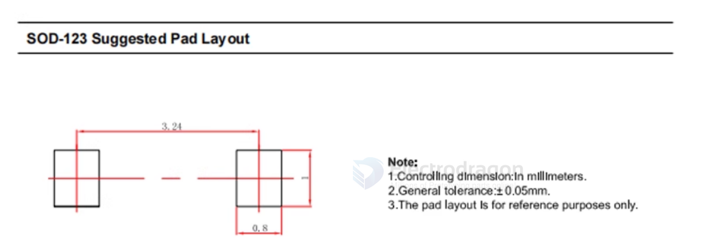
SOD-123
SOD-123 is a small SMD package used for diodes, transistors, and other components. It has a footprint of approximately 1.6mm x 0.8mm (0.063" x 0.031") and is commonly used in low-power applications.