soldering under microscope
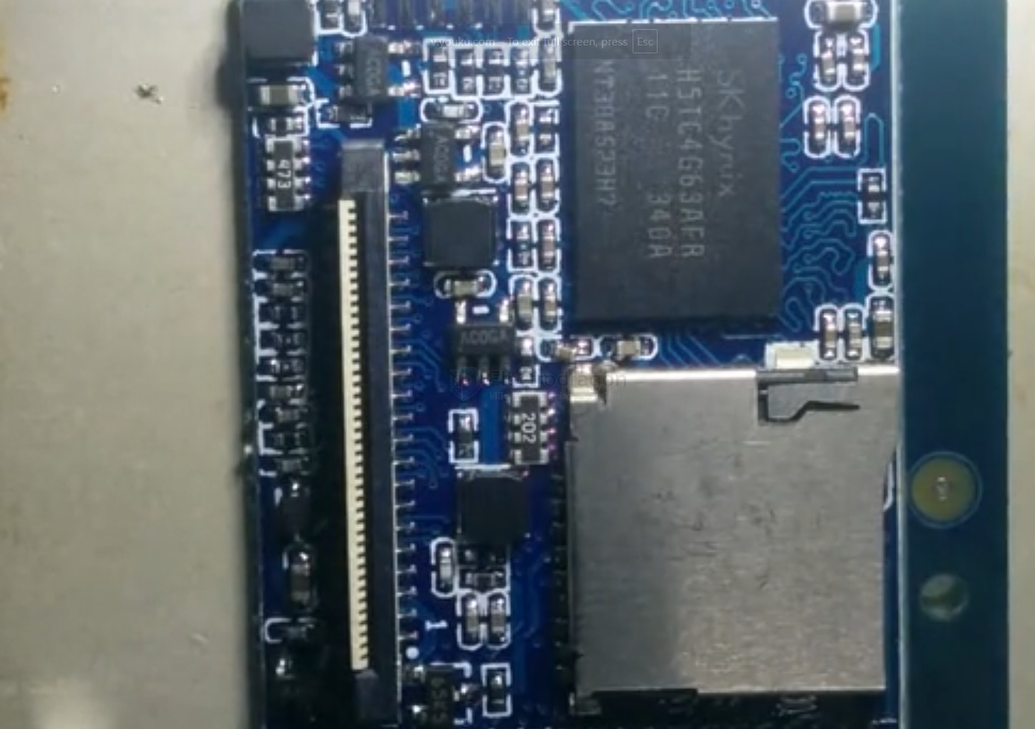
PCBA
- include extra assembly, files
PCBA Design
PCB-make-dat
make machine
PCB protection service
- for this module, consider add - Adhesive Solutions on PCBs - PCB-Adhesive-dat
- or layered plastic case layered-case-dat
- more simple soltuion - PMP1037-dat
Automated Methods to Check Complex Footprints (Unsoldered Pads)
E-Test is for the bare PCB (before assembly).
- It checks copper traces, vias, and pads for:
- Short circuits (unwanted connections between nets).
- Open circuits (broken or missing connections).
- Done by the PCB manufacturer using a flying probe tester or a bed-of-nails fixture.
- Ensures the bare board matches the Gerber/netlist before any components are soldered.
| Method | How It Works | Pros | Cons |
|---|---|---|---|
| Automated Optical Inspection (AOI) | High-resolution cameras scan PCB to compare against "golden board" or Gerber. Detects shorts, opens, mask issues, pad misalignment. | Fast, widely used in PCB fab & assembly. | Limited for hidden pads (BGA bottom side). |
| Flying Probe Test | Robotic probes touch each pad/net and check connectivity vs netlist. | No test fixture needed, flexible, high accuracy. | Slower than bed-of-nails, not good for high volume. |
| In-Circuit Test (ICT / Bed-of-Nails) | Custom test fixture presses spring pins into test pads, verifying continuity, isolation, resistance, etc. | Very fast, accurate, used for production. | Expensive setup, needs test points designed in. |
| X-Ray Inspection (AXI) | X-ray scans to detect hidden bridges, voids, and pad geometry (great for BGA/QFN). | Can see under packages, detects hidden issues. | Expensive equipment, slower than AOI. |
| Electrical Netlist Test (Bare Board E-Test) | PCB fab tests each board against Gerber netlist for shorts/opens using a flying probe. | Ensures PCB is correct before assembly. | Only checks copper nets, not mask/pad alignment. |
| Solder Paste Inspection (SPI) | 3D laser scan checks solder paste deposits on pads. | Ensures correct stencil printing before reflow. | Only useful after paste printing stage. |
| Coplanarity / Surface Profiling | Laser or white-light interferometer scans pads for height/flatness. | Ensures pads are level for fine-pitch ICs. | More common in IC packaging QA. |
Typical Workflow in Production
-
Bare PCB stage → Electrical netlist test + AOI.
-
Assembly stage (before soldering ICs) → AOI for pad/solder mask check, SPI for solder paste.
-
After soldering → AOI again + X-ray for BGA/QFN.
-
Final board → ICT (bed-of-nails) or flying probe for electrical verification.
👉 For prototyping / small batch, fabs usually run bare board E-test + AOI already.
👉 For hidden pad packages (QFN/BGA), the only real automated detection is X-ray.