chip info
module HDK == ESP-12F-DAT
common pins
| pin | name | GPIO | function | Note | note |
|---|---|---|---|---|---|
| 25 | U0_RXD | 3 | IO3 | I/O UART Rx during flash programming | |
| 26 | U0_TXD | 1 | IO1 | SPI_CS1 | I/O UART TX during flash programming; |
| 14 | IO2 | 2 | U1_TXD | Flash debug output | |
| 13 | MTDO | 15 | U0_RTS | HSPI_CS | |
| 18~23 | SDIO | ||||
| 8 | XPD_DCDC | IO16 | Deep-sleep wakeup (need to be connected to EXT_RSTB); GPIO16 |
Hardware SPI Pins (Default)
- MOSI (Master Out Slave In): GPIO13 (NodeMCU D7)
- MISO (Master In Slave Out): GPIO12 (NodeMCU D6)
- SCK (Serial Clock): GPIO14 (NodeMCU D5)
- CS/SS (Chip Select): GPIO15 (NodeMCU D8) - but you can use any GPIO pin for CS
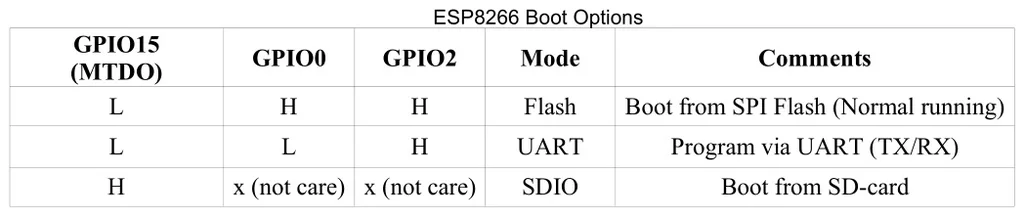
bootstrap
| pin | default boot | Against Mode | ESP-12F-dat | ESP-12S-dat | func |
|---|---|---|---|---|---|
| RESET | pull up + cap 0.1 UF | Reboot | ext. | int. | |
| EN | pull up | Reboot | ext. | int. | |
| IO0 | pull up | Flash Mode | ext. | int. | Boot mode control |
| IO2 | pull up | pull-up w/LED | pull-up w/LED | on-module LED | |
| GPIO15 | pull down | Fail into SDIO Mode | ext. | int. | MTDO |
- reference from chip datasheet section "Pin Definitions" Note part
ADC
(4. Peripheral Interface)
Hardware Design - The input voltage range is 0 to 1.0 V when TOUT is connected to external circuit.
Schematic
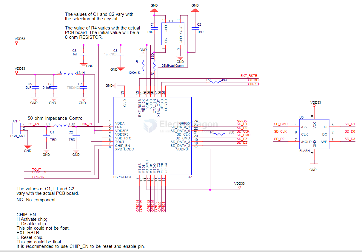
The ESP8266EX schematics include seven aspects:
• Power supply • Power-on sequence and reset • Flash • Crystal oscillator • RF • External resistor • UART
GPIO 16
❌ What GPIO16 Cannot Do
| Feature | Support | Notes |
|---|---|---|
| PWM (analogWrite) | ❌ No | GPIO16 does not support hardware PWM. |
| Interrupts (attachInterrupt) | ❌ No | Cannot be used for interrupts. |
| I²C / SPI / UART | ❌ No | Not multiplexed for any peripheral functions. |
| Analog input | ❌ No | ESP8266 has only one ADC (ADC0), not on GPIO16. |
| Open-drain / Pull-up/down | ❌ No | Limited internal resistor configuration. |
| Output during deep sleep | ⚠️ Caution | When used for deep sleep wake, it must not be driven externally. |
✅ What GPIO16 Can Do
| Feature | Support | Notes |
|---|---|---|
| Digital output | ✅ Yes | Use with digitalWrite(). |
| Digital input | ✅ Yes | Use with digitalRead(). |
| Deep sleep wake | ✅ Yes | Connect GPIO16 to RST to enable timed wake from deep sleep. |
interrrupt
✅ Recommended GPIOs for Interrupts
| GPIO | Usable for Interrupts? | Notes |
|---|---|---|
| GPIO0 | ✅ Yes | Must be HIGH at boot (pulled LOW enters flash mode) |
| GPIO2 | ✅ Yes | Must be HIGH at boot |
| GPIO4 | ✅ Yes | Safe |
| GPIO5 | ✅ Yes | Safe |
| GPIO12 | ✅ Yes | Safe |
| GPIO13 | ✅ Yes | Safe |
| GPIO14 | ✅ Yes | Safe |
peripherals
programmer and programming
DPR1150-dat - NWI1070-dat for ESP-01/01S
Batch Brogramming for ESP8266 modules, use OPM1095-dat and DPR1120-dat - https://t.me/electrodragon3/331
ESP8266 pins table
| pin | name | sytem | usage | custom | custom2 |
|---|---|---|---|---|---|
| 1 | VDDA | power. | |||
| 2 | LNA | Antenna-dat | |||
| 3 | VDD3P3 | power. | |||
| 4 | VDD3P3 | power. | |||
| 5 | VDD_RTC | x | |||
| 6 | TOUT | ADC-dat | |||
| 7 | CHIP_EN | ||||
| 8 | XPD_DCDC | IO16 | |||
| 9 | MTMS | IO14 | |||
| 10 | MTDI | IO12 | |||
| 11 | VDDPST | power. | |||
| 12 | MTCK | IO13 | |||
| 13 | MTDO | boot - L | IO15 | ||
| 14 | GPIO2 | boot - H | IO2 | ||
| 15 | GPIO0 | boot - H | IO0 | mod.led | |
| 16 | GPIO4 | IO4 | |||
| 17 | VDDPST | power. | |||
| 18 | SD_DATA_2 | flash | x-IO9 | ||
| 19 | SD_DATA_3 | flash | x-IO10 | ||
| 20 | SD_CMD | flash | x-IO11 | ||
| 21 | SD_CLK | flash | x-IO6 | ||
| 22 | SD_DATA_0 | flash | x-IO7 | ||
| 23 | SD_DATA_1 | flash | x-IO8 | ||
| 24 | GPIO5 | IO5 | |||
| 25 | U0RXD | UART | |||
| 26 | U0TXD | UART | |||
| 27 | XTAL_OUT | x | |||
| 28 | XTAL_IN | x | |||
| 29 | VDDD | power. | |||
| 30 | VDDA | power. | |||
| 31 | RES12K | x | |||
| 32 | EXT_RSTB | reset-dat | |||
| pad | GND | power. |
- XPD_DCDC - Deep-sleep wakeup (need to be connected to EXT_RSTB);