The ESP8089 module supports standard IEEE802.11 b/g/n protocols and a complete TCP/IP protocol stack. Hardware-wise, developers only need to communicate with an external MCU via the SPI/SDIO interface or the CPU AHB bridge interface.
The module supports energy-saving VoLP for fast switching between sleep/wake modes, adaptive wireless bias for low-power operation, front-end signal processing, fault isolation, and wireless coexistence features to eliminate interference from cellular/Bluetooth/802.11. It is widely used in home automation, security, smart appliances, wearables and remote controls, drones, OTT boxes, and industrial IoT.
Features
- Supports standard IEEE802.11 b/g/n protocols
- Supports Wi-Fi Direct (P2P), Miracast, SoftAP
- Built-in TCP/IP protocol stack
- Integrated TR switch, balun, LNA, power amplifier, and network matching
- Integrated PLL, voltage regulator, and power management components
- Up to +19dBm output power in 802.11b mode
- Leakage current less than 10uA
- Supports SDIO 2.0 and SPI interfaces
- STBC, 1x1 MIMO, 2x1 MIMO
- Frame aggregation with A-MPDU, A-MSDU, and 0.4us guard interval
- Wake, connect, and transmit packets within 22ms
- Standby power consumption less than 1.0mW (DTIM3)
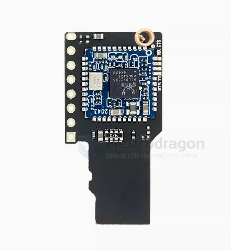
Board Features
PCB Specifications
- Layers: 4
- Dimensions: 13.5 × 13 × 1.8 mm
- Interface: Standard 1.5mm half-hole stamp pins, for direct PCB mounting
- Material: RF-specialized, high dielectric constant, low-loss substrate
Module Functional Characteristics
- Operating Voltage: 2.5V—3.6V
- Operating Temperature: -20℃ to 85℃
- Wi-Fi Version: 802.11 b/g/n
- Antenna: Stamp hole antenna interface
- Transmit Power: Up to +19dBm in 802.11b mode
- Communication Interface: SDIO
- 4-bit 25MHz SDIO v1.1
- 4-bit 50MHz SDIO v2.0
Module Pinout

| Pin | Name | Description |
|---|---|---|
| 1 | SD_D2 | SDIO_DATA_2 |
| 2 | SD_D3 | SDIO_DATA_3 |
| 3 | SD_CMD | SDIO_CMD |
| 4 | GND | Ground (must be connected to external controller GND) |
| 5 | SD_CLK | SDIO_CLK |
| 6 | SD_D0 | SDIO_DATA_0 |
| 7 | SD_D1 | SDIO_DATA_1 |
| 8 | VCC | Power supply DC: 2.5V—3.6V (recommend 3.3V, ≥500mA) |
| 9 | EN | Enable pin, active high (default pulled up), can be MCU controlled |
| 10 | GND | Ground |
| 11 | Wi-Fi_ANT | Antenna pin, for external antenna |
| 12 | GND | Ground |
| 13 | MTMS | General-purpose GPIO |
| 15 | MTDI | General-purpose GPIO |
PCB Layout Guidelines
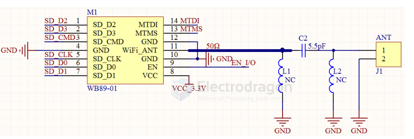
- Pin 11 (WiFi_ANT) output impedance is 50Ω. No matching required for the module, but it is recommended to reserve a π-type matching network for antenna tuning.
- Pin 9 (EN) is active high. Refer to the recommended circuit, or control via MCU I/O.
- Keep SDIO traces as short as possible.
- Avoid routing traces under the Wi-Fi module on the main board, and keep away from sensitive components (crystals, cameras, etc.).
- After soldering the module, perform antenna matching and RF performance testing.