no DVP display, only DVP-camera-dat
RGB Parallel Interface vs DVP Interface
| Feature | RGB Parallel Interface (Display MCU Interface) | DVP Interface (Digital Video Port, Camera) |
|---|---|---|
| Data Direction | MCU → Display | Camera → MCU |
| Data Lines | D0~D7 or D0~D15 (pixel data) | D0~D7 or D0~D9 (pixel data) |
| Control Signals | WR / RD / RS / CS / DE / HSYNC / VSYNC | PCLK / HREF / VSYNC |
| Timing | MCU-controlled writes (typical 8080 / 6800) | Camera outputs fixed pixel timing |
| Use Case | TFT LCD display | CMOS camera module |
| Interface Type | Parallel | Parallel |
| Similarity | Both use multi-line parallel pixel transfer | Both use multi-line parallel pixel transfer |
Summary:
- DVP is a parallel output interface from a camera; MCU or FPGA captures image data.
- The RGB parallel interface is a display input; MCU or FPGA drives the panel.
- They are electrically similar, but timing and purpose differ.
Can DVP Be Used as a Display Interface?
- Strictly speaking, DVP (Digital Video Port) was defined as a camera output interface for MCU/FPGA reception.
- However, in practice some low-resolution or embedded display modules can accept DVP-style input:
- These modules integrate a small controller that converts incoming DVP pixel timing into the panel drive.
- The MCU or FPGA sends pixel data following DVP timing directly to the module.
Characteristics
- Physical signals are similar: PCLK, VSYNC, HSYNC/HREF, data lines D0~Dn.
- Timing still follows DVP style (one pixel per PCLK edge).
- Common in low-resolution embedded TFT modules (e.g. 2.4", 2.8" TFT LCD).
Notes / Caveats
- You cannot treat a high-resolution raw TFT RGB panel as a DVP display module.
- The driving MCU/FPGA must generate DVP-like streaming timing, different from 8080/6800 register/data bus write cycles.
- Datasheets will usually state “DVP input” or “Camera interface for MCU” if such usage is supported.
Conclusion:
- DVP is fundamentally a camera (image sensor) interface.
- Some display modules are DVP-compatible, but you must adhere to DVP streaming timing and control behavior.
MIPI vs DVP Interface Comparison
| Feature | MIPI (DSI / CSI) | DVP (Digital Video Port) |
|---|---|---|
| Type | High-speed serial differential signaling | Parallel CMOS/TTL signaling |
| Data Lines | 1–4 (sometimes 8) differential lanes + clock | Multiple parallel data lines (8, 10, 12, 16 bits) |
| Clock | Embedded in protocol (Data lanes use DDR with strobe) | Separate dedicated pixel clock (PCLK) |
| Signal Standard | MIPI D-PHY / C-PHY (low-voltage differential) | CMOS/TTL single-ended logic |
| Data Rate | Up to several Gbps per lane | Typically < 150 MHz pixel clock |
| Wiring Complexity | Fewer wires (high-speed pairs) | Many wires (one per data bit + sync) |
| Pins | Very few (e.g., 4–10 total) | Many (e.g., 10–20+ total) |
| Sync Signals | Embedded in packet protocol | HSYNC, VSYNC required |
| Protocol Layer | Uses packet-based protocol (like networking) | Raw pixel data per clock |
| Power Consumption | Lower per bit transferred (but high-speed) | Higher due to many single-ended lines |
| Typical Use | Smartphones, tablets, high-res displays/cameras | Simple camera modules, low-cost LCDs |
| Example Devices | MIPI-DSI display panels, MIPI-CSI2 camera sensors | OV7670 camera, parallel RGB LCD panels |
DVP in the display context usually refers to the Digital Video Port interface. - parallel-display-dat It’s a parallel interface commonly used in cameras, simple LCDs, or microcontroller-driven displays.
How it works
- Transfers pixel data in parallel (8, 16, or 24 data lines, depending on color depth).
- Uses synchronization signals:
- HSYNC (Horizontal Sync) – signals the start of a new line
- VSYNC (Vertical Sync) – signals the start of a new frame
- PCLK (Pixel Clock) – latches each pixel’s data
- Can work with formats like RGB565, RGB888, or YUV422.
Key Characteristics
- Simple protocol – no complex packetization (unlike MIPI-DSI).
- Lower speed – parallel clock typically in the tens of MHz.
- More pins needed – due to multiple parallel data lines.
- Used in MCUs and simple SoCs – no need for high-speed serializers.
Common Uses
- Cheap TFT LCD modules with MCU controllers
- CMOS camera modules with parallel output
- Low-resolution displays in industrial or hobby projects
Comparison (DVP vs MIPI-DSI)
| Feature | DVP (Digital Video Port) | MIPI-DSI |
|---|---|---|
| Data Transfer | Parallel (8–24 data lines) | High-speed serial (2–4 lanes) |
| Speed | Tens of MHz | Hundreds of MHz to Gbps |
| Pin Count | High | Low |
| Complexity | Simple | Complex, packetized |
| Use Case | Simple displays, cameras | High-res smartphone/tablet displays |
SCH
8-bit Y2 ~ Y9 // HSYNC + VSYNC + PCLK + XCLK + SCL + SDA + **RST
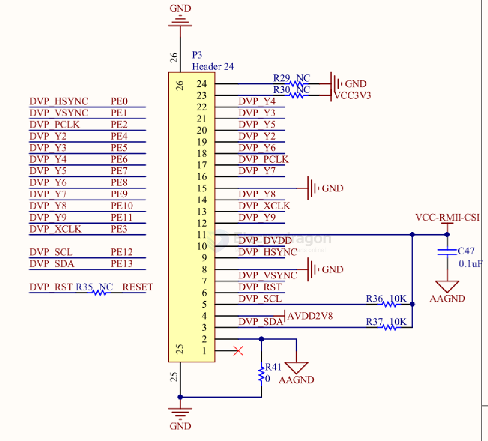
DVP Display 22-Pin Interface
6 bit version
| Pin No. | Symbol | Description |
|---|---|---|
| 1 | VCC | Power supply |
| 2 | GND | Ground |
| 3 | RST | Reset |
| 4 | CS | Chip select |
| 5 | SCL | Serial clock |
| 6 | VS | Vertical sync |
| 7 | HS | Horizontal sync |
| 8 | DE | Data enable |
| 9 | DLCK | Data clock (pixel clock) |
| 10 | SDA | Serial data |
| 11 | K | Backlight control (LEDK) |
| 12 | A | Backlight control (LEDA) |
| 13 | D0 | Data bit 0 |
| 14 | D1 | Data bit 1 |
| 15 | D2 | Data bit 2 |
| 16 | D3 | Data bit 3 |
| 17 | D4 | Data bit 4 |
| 18 | D5 | Data bit 5 |
| 19 | NC | - |
| 20 | NC | - |
| 21 | NC | - |
| 22 | NC | - |