Dynamic Random Access Memory (DRAM) is a type of volatile memory that stores data in capacitors within integrated circuits.
Key Characteristics:
- Dynamic: Requires periodic refreshing (every few milliseconds) because capacitors leak charge over time
- Volatile: Data is lost when power is removed
- Random Access: Any memory location can be accessed directly in any order
- High Density: Can store more data per chip compared to SRAM
- Lower Cost: Cheaper per bit than SRAM due to simpler cell structure
How DRAM Works:
- Storage Cell: Each bit is stored as charge in a tiny capacitor
- Transistor Switch: Controls access to the capacitor
- Refresh Cycle: Memory controller periodically reads and rewrites data to maintain charge
- Row/Column Addressing: Uses multiplexed addressing to reduce pin count
Types of DRAM:
- SDRAM: Synchronous DRAM - synchronized with system clock
- DDR SDRAM: Double Data Rate - transfers data on both clock edges
- DDR2/DDR3/DDR4/DDR5: Successive generations with higher speeds and lower power
- LPDDR: Low Power DDR for mobile devices
- GDDR: Graphics DDR for video cards
Common Applications:
- System RAM in computers and smartphones
- Frame buffers in graphics cards
- Buffer memory in networking equipment
- Temporary storage in embedded systems
DRAM vs Other Memory Types:
| Type | Speed | Cost | Density | Volatility | Refresh |
|---|---|---|---|---|---|
| DRAM | Medium | Low | High | Volatile | Required |
| SRAM | High | High | Low | Volatile | Not Required |
| Flash | Low | Medium | High | Non-volatile | Not Required |
| EEPROM | Very Low | High | Low | Non-volatile | Not Required |
DRAM chip
PMS307416A == Synchronous Dynamic RAM == 2048K Words x 16 Bits x 4 Banks (128-MBIT)
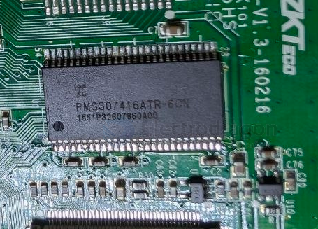
Features
- Clock frequency: 166, 133 MHz
- Fully synchronous; all signals referenced to a positive clock edge
- Four banks operation
- Single 3.3V power supply
- LVTTL interface
- Programmable burst length -- (1, 2, 4, 8, full page)
- Programmable burst sequence: Sequential/Interleave
- 4096 refresh cycles every 64 ms
- Random column address every clock cycle Programmable /CAS latency (2, 3 clocks)
- Burst read/write and burst read/single write operations capability
- Burst termination by burst stop and precharge command
- Byte controlled by LDQM and UDQM
- Packages 400-mil 54-pin TSOP-II
- Lead-free package
https://www.scribd.com/document/744434108/PMS307416A
8Gb: x4, x8, x16 DDR4 SDRAM - DDR4 SDRAM = MT40A2G4 = MT40A1G8 = MT40A512M16