Based on powerbus slave chip PB331.
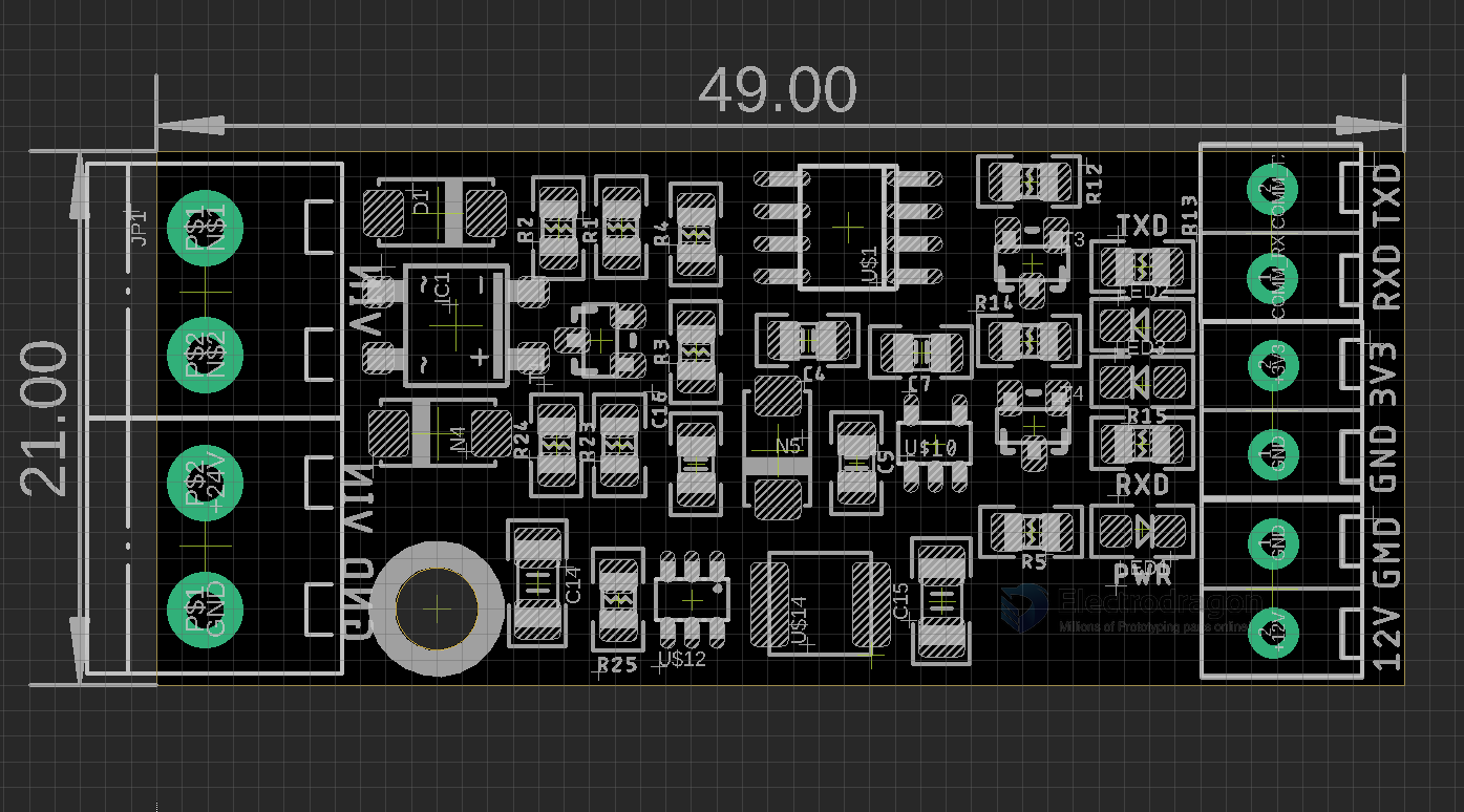
dimension
Function map
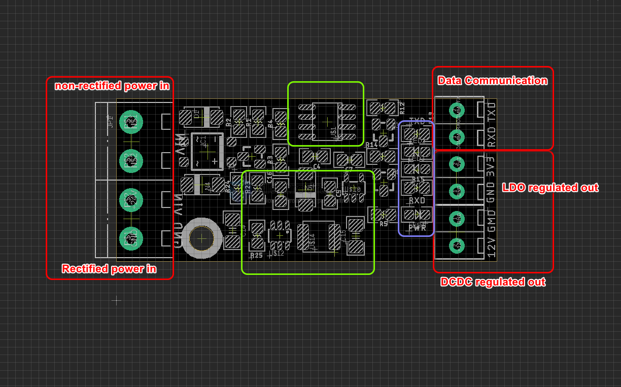
- left top terminal - no direction power input
- left bottom terminal - 24V - GND
- right top terminal - serial input and output
- right middle terminal - 3.3V - GND on board regulator output
-
right bottom terminal - 12V - GND on board DCDC switcher output
-
based on option 401: DCDC-dat
- based on option 231: LDO-dat